Digital Logic

Community
Digital Logic
2078 Boards
Section A
Answer any two questions.
1
Design the sequential circuit with respect to the following state diagram using J-K flip flops.
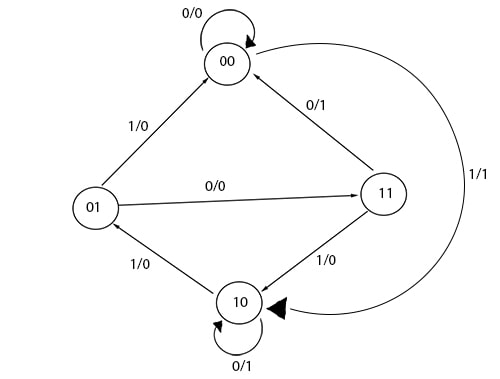
10
Connect with us on Discord to become a contributor.
2
Implement F = Σ(0, 2, 3, 4, 7) using
Multiplexer
Decoder
PLA
10
Connect with us on Discord to become a contributor.
3
Difference between synchronous and asynchronous counter. Design mode-7 synchronous counter using T-flip flop. Show necessary truth tables and k-maps.
10
Connect with us on Discord to become a contributor.
Section B
Answer any eight questions.
4
Provide one example where shift right operation can be used. Explain parallel-in-parallel-out register.
5
-
Shift Right Operation Example:
Shift right operation is commonly used for efficient integer division by powers of two. For instance, shifting a binary number right by one position is equivalent to dividing the number by 2. This is a fast operation often implemented directly by hardware. -
Parallel-In-Parallel-Out (PIPO) Register:
A Parallel-In-Parallel-Out (PIPO) register is a type of digital register where data bits are loaded into the register simultaneously (in parallel) and are also read out from the register simultaneously (in parallel). It typically consists of a series of D flip-flops, one for each bit, with common clock and clear inputs. Each flip-flop's data input (D) is connected to a corresponding parallel input line, and its output (Q) provides a corresponding parallel output line. This configuration allows for the instantaneous storage and retrieval of a complete multi-bit word.
5
Carry out the following task
Preform 1’s complement subtraction 110101 – 100101
Represent decimal number 0.125 into its binary form
5
1's Complement Subtraction: 110101 – 100101
- Step 1: Identify Minuend (A) and Subtrahend (B)
- A = 110101
- B = 100101
- Step 2: Find the 1's complement of the subtrahend (B')
- B' = 011010
- Step 3: Add A to B'
110101 (A) + 011010 (B') ---------- 1001111 (Sum) - Step 4: Check for End-Around Carry
- An end-around carry of '1' is generated.
- Step 5: Add the End-Around Carry to the Sum
001111 (Sum without carry) + 1 (End-around carry) ---------- 010000 - Result: The result of the 1's complement subtraction is 010000.
Decimal to Binary Conversion: 0.125
- Step 1: Multiply the fractional part by 2
- 0.125 * 2 = 0.25 (Integer part = 0)
- Step 2: Multiply the new fractional part by 2
- 0.25 * 2 = 0.50 (Integer part = 0)
- Step 3: Multiply the new fractional part by 2
- 0.50 * 2 = 1.00 (Integer part = 1)
- Step 4: Collect the integer parts from top to bottom
- 0.001
- Result: The binary representation of decimal 0.125 is 0.001.
6
Derive the Boolean expression for sum and carry of half adder. Draw its combinational circuit. Implement it using only NAND gates.
5
Connect with us on Discord to become a contributor.
7
Express the Boolean function F = x + yz as product of max-terms.
5
To express the Boolean function F = x + yz as a product of max-terms, first identify the min-terms where the function is true, and then find the complementary min-terms which correspond to the max-terms.
-
Standardize the function with all variables:
- F = x + yz
- Since there are three variables (x, y, z), each term must include all variables in their true or complemented form.
- x = x(y + y')(z + z') = (xy + xy')(z + z') = xyz + xyz' + xy'z + xy'z'
- yz = yz(x + x') = xyz + x'yz
-
Combine and simplify to find sum of min-terms:
- F = (xyz + xyz' + xy'z + xy'z') + (xyz + x'yz)
- Remove duplicate term (xyz):
- F = xyz + xyz' + xy'z + xy'z' + x'yz
-
List the corresponding min-terms (m_i):
- xyz (111) = m₇
- xyz' (110) = m₆
- xy'z (101) = m₅
- xy'z' (100) = m₄
- x'yz (011) = m₃
- Therefore, F = Σm(3, 4, 5, 6, 7)
-
Identify the missing min-terms, which correspond to the max-terms (M_i) where F is false:
- For 3 variables, the possible min-terms are m₀ to m₇.
- The missing min-terms are m₀, m₁, m₂.
- Therefore, F = ΠM(0, 1, 2)
-
Write the product of max-terms:
- M₀ (000) = x + y + z
- M₁ (001) = x + y + z'
- M₂ (010) = x + y' + z
- F = (x + y + z)(x + y + z')(x + y' + z)
8
Minimize the Boolean function Boolean function using K-map
F(A, B, C, D) = Σ(0, 1, 3, 5, 7, 8, 9, 11, 13, 15)
5
Connect with us on Discord to become a contributor.
9
What are the practical implementations of up counter? Explain Binary ripple counter.
5
Practical Implementations of Up Counters:
- Digital Clocks and Timers: Used to count seconds, minutes, and hours in real-time clock applications or to measure time intervals.
- Frequency Dividers: By using a counter that counts up to a specific number and then resets, the input frequency can be divided by that number.
- Event Counters: For counting occurrences of specific events, such as products on an assembly line, pulses from a sensor, or clock cycles in a processor.
- Address Generators: In memory systems, counters can generate sequential memory addresses for data access.
- Analog-to-Digital Converters (ADCs): In some ADC architectures (e.g., ramp ADCs), an up counter is used to generate a digital value that is compared against an analog input.
Binary Ripple Counter Explanation:
A binary ripple counter is an asynchronous counter where the output of one flip-flop serves as the clock input for the subsequent flip-flop.
- Structure: It is typically constructed using multiple J-K flip-flops or T flip-flops, with each flip-flop configured in toggle mode (J=K=1 or T=1). The flip-flops are connected in series.
- Operation:
- The external clock signal is applied only to the clock input of the first flip-flop (representing the Least Significant Bit, LSB).
- The output (Q) of the first flip-flop toggles on each active edge of the external clock.
- This Q output then acts as the clock input for the second flip-flop, causing it to toggle at half the frequency of the first.
- This process continues down the chain, with each successive flip-flop toggling at half the frequency of the preceding one.
- The propagation delay through each flip-flop results in a sequential change in state that "ripples" through the counter, hence the name.
- Characteristics: Simple to design and implement, but suffers from cumulative propagation delays which limit its maximum operating speed and can lead to transient invalid states (glitches) during state transitions.
10
Design a combinational circuit with three inputs and one output. The output is 1 when the binary value of the inputs is an odd number.
5
Connect with us on Discord to become a contributor.
11
Differentiate between PLA and PAL. Explain 4-bit magnitude comparator
5
Connect with us on Discord to become a contributor.
12
Write short notes on (Any Two)
Negative Logic
CMOS
EBCDIC
5
Negative Logic
- A convention for interpreting logic levels where a higher voltage level represents a logic '0' (FALSE), and a lower voltage level represents a logic '1' (TRUE).
- Contrasts with positive logic, where a higher voltage is '1' and a lower voltage is '0'.
- Under negative logic, the functionality of basic gates changes; for example, a positive logic AND gate behaves as a negative logic OR gate.
- Used in specific digital systems or for certain circuit design simplifications.
CMOS
- Stands for Complementary Metal-Oxide-Semiconductor, a technology for constructing integrated circuits.
- Utilizes pairs of complementary (P-type and N-type) MOSFETs to implement logic gates and other digital circuits.
- Characterized by extremely low static power dissipation because in steady-state operation (when the circuit is not switching), one transistor in the complementary pair is always off, blocking the current path from Vcc to ground.
- Offers high noise immunity, a wide operating voltage range, and high integration density, making it the dominant technology for modern microprocessors, memory, and custom logic chips.