Digital Logic
Community
Digital Logic
2074 Boards
Section A
Answer any two questions.
1
Implement the following Functions F= Σ (0,3,5,6,7) using
Decoder
Multiplexer
PLA
10
Connect with us on Discord to become a contributor.
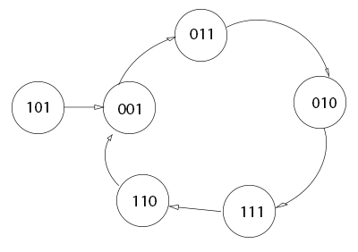
2
Differentiate between PAL and PLA. Design a counter as shown in the state diagram below
10
Connect with us on Discord to become a contributor.
3
Draw a block diagram, truth table and logic circuit of 1*16 Demultiplexer and explain its working principle.
10
Connect with us on Discord to become a contributor.
Section B
Answer any eight questions.
4
Perform the arithmetic operation (+42)+(-13) and (-42)-(-13) in binary using the signed -2’s-complement representation for negative numbers.
5
The operations are performed using 7-bit signed 2's complement representation. The range for 7-bit signed 2's complement is -64 to +63, which accommodates the given numbers.
1. Binary Representation:
- +42:
- Decimal 42 = 0101010₂
- In 7-bit signed 2's complement: 0101010
- -13:
- Decimal 13 = 0001101₂
- 1's complement of +13 (0001101): 1110010
- Add 1 for 2's complement: 1110010 + 1 = 1110011
- -42:
- Decimal 42 = 0101010₂
- 1's complement of +42 (0101010): 1010101
- Add 1 for 2's complement: 1010101 + 1 = 1010110
2. Arithmetic Operations:
(a) (+42) + (-13)
- Operation: Add the 2's complement representations.
- Calculation:
0101010 (+42) + 1110011 (-13) --------- (1)0011101 (Carry out ignored for 7-bit result) - Result: 0011101
- Verification: 0011101₂ = 16 + 8 + 4 + 1 = 29₁₀.
- (+42) + (-13) = +29.
(b) (-42) - (-13)
- This operation is equivalent to (-42) + (+13) in 2's complement.
- We need the 2's complement of -13, which is +13.
- +13 in 7-bit signed 2's complement: 0001101
- Calculation:
1010110 (-42) + 0001101 (+13) --------- 1100011 - Result: 1100011
- Verification: The MSB is 1, so it's a negative number.
- Take 2's complement of 1100011 to find its magnitude:
- 1's complement: 0011100
- Add 1: 0011100 + 1 = 0011101
- 0011101₂ = 29₁₀.
- Therefore, 1100011 represents -29₁₀.
- Take 2's complement of 1100011 to find its magnitude:
- (-42) - (-13) = -42 + 13 = -29.
- Verification: The MSB is 1, so it's a negative number.
5
Express the complement of the following function in sum of min-terms.
F(A, B, C, D) = Σ(0, 2, 6, 11, 13, 14)
5
Connect with us on Discord to become a contributor.
6
Reduce the following function using k-map F = wxy + yz + xy’z + x’y
5
Connect with us on Discord to become a contributor.
7
Design a combinational circuit with three inputs and six outputs. The output binary number should be the square of the input binary number.
5
Connect with us on Discord to become a contributor.
8
Design a 5 x 32 decoder with four 3 x 8 decoder with enable and one 2 x 4 decoder. Use block diagrams only.
5
Connect with us on Discord to become a contributor.
9
Design and explain the Decimal adder with truth table and suitable diagram.
5
Connect with us on Discord to become a contributor.
10
Explain shift register with parallel load. Highlight on its practical implications.
5
A shift register with parallel load is a digital circuit capable of performing both serial shifting of data and simultaneous parallel loading of data into its internal flip-flops. It typically includes control inputs to select between these operational modes.
Operation:
- Parallel Load Mode: When the control signal (e.g., Load) is active, data present on the parallel input lines is loaded into all flip-flops of the register simultaneously on the clock edge.
- Shift Mode: When the control signal (e.g., Shift) is active, data is shifted serially from one flip-flop to the next on each clock edge, similar to a standard shift register. Data can be shifted in or out serially.
Practical Implications:
- Data Conversion: Facilitates both Serial-to-Parallel (SIPO) and Parallel-to-Serial (PISO) data conversion, essential in communication systems and data processing.
- Data Manipulation: Useful for temporary data storage, data alignment, and reordering of bit sequences.
- Bus Interface: Can act as an interface between parallel data buses and serial data lines, commonly found in microcontrollers and peripheral devices.
- Pattern Generation: Can be configured to generate specific bit patterns or sequences.
11
Explain master slave J-K flipflop.
5
Connect with us on Discord to become a contributor.
12
Write short notes on (any two):
State diagram
De-Morgan’s theorem
TTL
5
De-Morgan’s Theorem
De-Morgan’s theorems are a pair of transformation rules in Boolean algebra that are fundamental for simplifying Boolean expressions and for converting between different forms of logic gates (e.g., NAND to OR, NOR to AND). They state that:
- The complement of a product of variables is equal to the sum of the complements of the variables.
- $\overline{A \cdot B} = \overline{A} + \overline{B}$
- This implies that a NAND gate behaves like an OR gate with inverted inputs.
- The complement of a sum of variables is equal to the product of the complements of the variables.
- $\overline{A + B} = \overline{A} \cdot \overline{B}$
- This implies that a NOR gate behaves like an AND gate with inverted inputs.
These theorems are extensively used in digital circuit design for logic minimization and for implementing circuits using universal gates (NAND or NOR gates exclusively).
TTL (Transistor-Transistor Logic)
Transistor-Transistor Logic (TTL) is a family of digital integrated circuits constructed using bipolar junction transistors (BJTs). It was a dominant technology for digital logic circuits for several decades.
Key characteristics of TTL:
- Construction: Employs multiple-emitter transistors at the input stage, followed by a phase splitter and a totem-pole output stage.
- Voltage Levels: Operates with specific voltage ranges for logic HIGH and LOW states, typically:
- Output HIGH (V_OH_): > 2.4V (min)
- Output LOW (V_OL_): < 0.4V (max)
- Input HIGH (V_IH_): > 2V (min)
- Input LOW (V_IL_): < 0.8V (max)
- Power Dissipation: Generally higher compared to CMOS, and increases with operating frequency.
- Speed: Offers good switching speeds, with propagation delays in the range of nanoseconds. Various sub-families (e.g., Schottky TTL, Low-Power Schottky TTL) were developed to optimize speed and power consumption.
- Noise Margin: Typically good noise immunity due to distinct voltage thresholds.
TTL devices are widely used in general-purpose digital applications, interfacing with microprocessors, and building combinational and sequential logic circuits.